
Taiwan Semiconductor Manufacturing Company (NYSE: TSM) has officially ushered in the next era of computing, confirming that its 2nm (N2) process node has reached high-volume manufacturing (HVM) as of January 2026. This milestone represents more than just a reduction in transistor size; it marks the company’s first transition to Nanosheet Gate-All-Around (GAA) architecture, a fundamental shift in how chips are built. With early yield rates stabilizing between 65% and 75%, TSMC is effectively outpacing its rivals in the commercialization of the most advanced silicon on the planet.
The timing of this announcement is critical, as the global demand for generative AI and high-performance computing (HPC) continues to outstrip supply. By successfully ramping up N2 production at its Hsinchu and Kaohsiung facilities, TSMC has secured its position as the primary engine for the next generation of AI accelerators and consumer electronics. Simultaneously, the company’s massive expansion in Arizona is redefining the geography of the semiconductor industry, evolving from a satellite project into a multi-hundred-billion-dollar "gigafab" cluster that promises to bring the cutting edge of manufacturing to U.S. soil.
The N2 Leap: Nanosheet GAA and the End of the FinFET Era
The transition to the N2 node marks the definitive end of the FinFET (Fin Field-Effect Transistor) era, which has governed the industry for over a decade. The new Nanosheet GAA architecture involves a design where the gate surrounds the channel on all four sides, providing superior electrostatic control. This technical leap allows for a 10% to 15% increase in speed at the same power level compared to the preceding N3E node, or a staggering 25% to 30% reduction in power consumption at the same speed. Furthermore, TSMC’s "NanoFlex" technology has been integrated into the N2 design, allowing chip architects to mix and match different nanosheet cell heights within a single block to optimize specifically for high speed or high density.
Initial reactions from the AI research and hardware communities have been overwhelmingly positive, particularly regarding TSMC’s yield stability. While competitors have struggled with the transition to GAA, TSMC’s conservative "GAA-first" approach—which delayed the introduction of Backside Power Delivery (BSPD) until the subsequent N2P node—appears to have paid off. By focusing on transistor architecture stability first, the company has achieved yields that are reportedly 15% to 20% higher than those of Samsung (KRX:005930) at a comparable stage of development. This reliability is the primary factor driving the "raging" demand for N2 capacity, with tape-outs estimated to be 1.5 times higher than they were for the 3nm cycle.
Technical specifications for N2 also highlight a 15% to 20% increase in logic-only chip density. This density gain is vital for the massive language models (LLMs) of 2026, which require increasingly large amounts of on-chip SRAM and logic to handle trillion-parameter workloads. Industry experts note that while Intel (NASDAQ: INTC) has achieved an architectural lead by shipping its "PowerVia" backside power delivery in its 18A node, TSMC’s N2 remains the density and volume king, making it the preferred choice for the mass-market production of flagship mobile and AI silicon.
The Customer Gold Rush: Apple, Nvidia, and the Fight for Silicon Supremacy
The battle for N2 capacity has created a clear hierarchy among tech giants. Apple (NASDAQ: AAPL) has once again secured its position as the lead customer, reportedly booking over 50% of the initial 2nm capacity. This silicon will power the upcoming A20 chip for the iPhone 18 Pro and the M6 family of processors, giving Apple a significant efficiency advantage over competitors still utilizing 3nm variants. By being the first to market with Nanosheet GAA in a consumer device, Apple aims to further distance itself from the competition in terms of on-device AI performance and battery longevity.
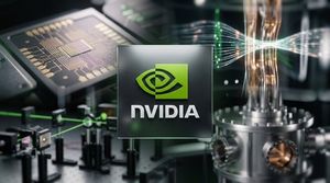
Nvidia (NASDAQ: NVDA) is the second major beneficiary of the N2 ramp. As the dominant force in the AI data center market, Nvidia has shifted its roadmap to utilize 2nm for its next-generation architectures, codenamed "Rubin Ultra" and "Feynman." These chips are expected to leverage the N2 node’s power efficiency to pack even more CUDA cores into a single thermal envelope, addressing the power-grid constraints that have begun to plague global data center expansion. The shift to N2 is seen as a strategic necessity for Nvidia to maintain its lead over challengers like AMD (NASDAQ: AMD), which is also vying for N2 capacity for its Instinct line of accelerators.
Even Intel, traditionally a rival in the foundry space, has reportedly turned to TSMC’s N2 node for certain compute tiles in its "Nova Lake" architecture. This multi-foundry strategy highlights the reality of the 2026 landscape: TSMC’s capacity is so vital that even its direct competitors must rely on it to stay relevant in the high-performance PC market. Meanwhile, Qualcomm (NASDAQ: QCOM) and MediaTek are locked in a fierce bidding war for the remaining N2 and N2P capacity to power the flagship smartphones of late 2026, signaling that the mobile industry is ready to fully embrace the GAA transition.
Arizona’s Transformation: The Rise of a Global Chip Hub
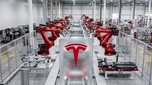
The expansion of TSMC’s Arizona site, known as Fab 21, has reached a fever pitch. What began as a single-factory initiative has blossomed into a planned complex of six logic fabs and advanced packaging facilities. As of January 2026, Fab 21 Phase 1 (4nm) is fully operational and shipping Blackwell-series GPUs for Nvidia. Phase 2, which will focus on 3nm production, is currently in the "tool move-in" phase with production expected to commence in 2027. Most importantly, construction on Phase 3—the dedicated 2nm and A16 facility—is well underway, following a landmark $250 billion total investment commitment supported by the U.S. CHIPS Act and a new U.S.-Taiwan trade agreement.
This expansion represents a seismic shift in the semiconductor supply chain. By fast-tracking a local Chip-on-Wafer-on-Substrate (CoWoS) packaging facility in Arizona, TSMC is addressing the "packaging bottleneck" that has historically required chips to be sent back to Taiwan for final assembly. This move ensures that the entire lifecycle of an AI chip—from wafer fabrication to advanced packaging—can now happen within the United States. The recent acquisition of an additional 900 acres in Phoenix further signals TSMC's long-term commitment to making Arizona a "Gigafab" cluster rivaling its operations in Tainan and Hsinchu.
However, the expansion is not without its challenges. The geopolitical implications of this "silicon shield" moving partially to the West are a constant topic of debate. While the U.S. gains significant supply chain security, some analysts worry about the potential dilution of TSMC’s operational efficiency as it manages a massive global workforce. Nevertheless, the presence of 4nm, 3nm, and soon 2nm manufacturing in the U.S. represents the most significant repatriation of advanced technology in modern history, fundamentally altering the strategic calculus for tech giants and national governments alike.
The Road to Angstrom: N2P, A16, and the Future of Logic
Looking beyond the current N2 launch, TSMC is already laying the groundwork for the "Angstrom" era. The enhanced version of the 2nm node, N2P, is slated for volume production in late 2026. This variant will introduce Backside Power Delivery (BSPD), a feature that decouples the power delivery network from the signal routing on the wafer. This is expected to provide an additional 5% to 10% gain in power efficiency and a significant reduction in voltage drop, addressing the "power wall" that has hindered mobile chip performance in recent years.
Following N2P, the company is preparing for its A16 node, which will represent the 1.6nm class of manufacturing. Experts predict that A16 will utilize even more exotic materials and High-NA EUV (Extreme Ultraviolet) lithography to push the boundaries of physics. The applications for these nodes extend far beyond smartphones; they are the prerequisite for the "Personal AI" revolution, where every device will have the local compute power to run sophisticated, autonomous agents without relying on the cloud.
The primary challenges on the horizon are the spiraling costs of design and manufacturing. A single 2nm tape-out can cost hundreds of millions of dollars, potentially pricing out smaller startups and consolidating power further into the hands of the "Magnificent Seven" tech companies. However, the rise of custom silicon—where companies like Microsoft (NASDAQ: MSFT) and Amazon (NASDAQ: AMZN) design their own N2 chips—suggests that the market is finding new ways to fund these astronomical development costs.
A New Era of Silicon Dominance
The successful ramp of TSMC’s 2nm N2 node and the massive expansion in Arizona mark a definitive turning point in the history of the semiconductor industry. TSMC has proven that it can manage the transition to GAA architecture with higher yields than its peers, effectively maintaining its role as the world’s indispensable foundry. The "GAA Race" of the early 2020s has concluded with TSMC firmly in the lead, while Intel has emerged as a formidable second player, and Samsung struggles to find its footing in the high-volume market.
For the AI industry, the readiness of 2nm silicon means that the exponential growth in model complexity can continue for the foreseeable future. The chips produced on N2 and its variants will be the ones that finally bring truly conversational, multimodal AI to the pockets of billions of users. As we look toward the rest of 2026, the focus will shift from "can it be built" to "how fast can it be shipped," as TSMC works to meet the insatiable appetite of a world hungry for more intelligence, more efficiency, and more silicon.
This content is intended for informational purposes only and represents analysis of current AI developments.
TokenRing AI delivers enterprise-grade solutions for multi-agent AI workflow orchestration, AI-powered development tools, and seamless remote collaboration platforms.
For more information, visit https://www.tokenring.ai/.