
As the calendar turns to late 2025, the semiconductor industry is witnessing its most profound architectural shift in over a decade. The arrival of Backside Power Delivery (BSPD), spearheaded by Intel Corporation (NASDAQ: INTC) and its proprietary PowerVia technology, has fundamentally altered the physics of chip design. By physically separating power delivery from signal routing, Intel has solved a decade-long "traffic jam" on the silicon wafer, providing a critical performance boost just as the demand for generative AI reaches its zenith.
This breakthrough is not merely an incremental improvement; it is a total reimagining of how electricity reaches the billions of transistors that power modern AI models. While traditional chips struggle with electrical interference and "voltage drop" as they shrink, PowerVia allows for more efficient power distribution, higher clock speeds, and significantly denser logic. For Intel, this represents a pivotal moment in its "five nodes in four years" strategy, potentially reclaiming the manufacturing crown from long-time rival Taiwan Semiconductor Manufacturing Company (NYSE: TSM).
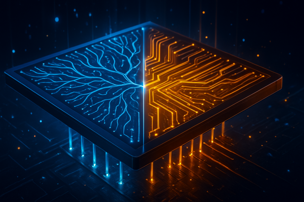
Unclogging the Silicon Arteries: The PowerVia Advantage
For nearly fifty years, chips have been built like a layer cake, with transistors at the bottom and all the wiring—both for data signals and power—layered on top. As transistors shrank to the "Angstrom" scale, these wires became so crowded that they began to interfere with one another. Power lines, which are relatively bulky, would block the path of delicate signal wires, leading to a phenomenon known as "crosstalk" and causing significant voltage drops (IR drop) as electricity struggled to navigate the maze. Intel’s PowerVia solves this by moving the entire power delivery network to the "backside" of the silicon wafer, leaving the "front side" exclusively for data signals.
Technically, PowerVia achieves this through the use of nano-Through Silicon Vias (nTSVs). These are microscopic vertical tunnels that pass directly through the silicon substrate to connect the backside power layers to the transistors. This approach eliminates the need for power to travel through 10 to 20 layers of metal on the front side. By shortening the path to the transistor, Intel has successfully reduced IR drop by nearly 30%, allowing transistors to switch faster and more reliably. Initial data from Intel’s 18A node, currently in high-volume manufacturing, shows frequency gains of up to 6% at the same power level compared to traditional front-side designs.
Beyond speed, the removal of power lines from the front side has unlocked a massive amount of "real estate" for logic. Chip designers can now pack transistors much closer together, achieving density improvements of up to 30%. This is a game-changer for AI accelerators, which require massive amounts of logic and memory to process large language models. The industry response has been one of cautious optimism followed by rapid adoption, as experts recognize that BSPD is no longer a luxury, but a necessity for the next generation of high-performance computing.
A Two-Year Head Start: Intel 18A vs. TSMC A16
The competitive landscape of late 2025 is defined by a rare "first-mover" advantage for Intel. While Intel’s 18A node is already powering the latest "Panther Lake" consumer chips and "Clearwater Forest" server processors, TSMC is still in the preparation phase for its own BSPD implementation. TSMC has opted to skip a basic backside delivery on its 2nm node, choosing instead to debut an even more advanced version, called Super PowerRail, on its A16 (1.6nm) process. However, A16 is not expected to reach high-volume production until the second half of 2026, giving Intel a roughly 1.5 to 2-year lead in the commercial application of this technology.
This lead has already begun to shift the strategic positioning of major AI chip designers. Companies that have traditionally relied solely on TSMC, such as NVIDIA Corporation (NASDAQ: NVDA) and Apple Inc. (NASDAQ: AAPL), are now closely monitoring Intel's foundry yields. Intel’s 18A yields are currently reported to be stabilizing between 60% and 70%, a healthy figure for a node of this complexity. The pressure is now on TSMC to prove that its Super PowerRail—which connects power directly to the transistor’s source and drain rather than using Intel's nTSV method—will offer superior efficiency that justifies the wait.
For the market, this creates a fascinating dynamic. Intel is using its manufacturing lead to lure high-profile foundry customers who are desperate for the power efficiency gains that BSPD provides. Microsoft Corporation (NASDAQ: MSFT) and Amazon.com, Inc. (NASDAQ: AMZN) have already signed on to use Intel’s advanced nodes for their custom AI silicon, such as the Maia 2 and Trainium 2 chips. This disruption to the existing foundry hierarchy could lead to a more diversified supply chain, reducing the industry's heavy reliance on a single geographic region for the world's most advanced chips.
Powering the AI Infrastructure: Efficiency at Scale
The wider significance of Backside Power Delivery cannot be overstated in the context of the global AI energy crisis. As data centers consume an ever-increasing share of the world’s electricity, the 15-20% performance-per-watt improvement offered by PowerVia is a critical sustainability tool. For hyperscale cloud providers, a 20% reduction in power consumption translates to hundreds of millions of dollars saved in cooling costs and electricity bills. BSPD is effectively "free performance" that helps mitigate the thermal throttling issues that have plagued high-wattage AI chips like NVIDIA's Blackwell series.
Furthermore, BSPD enables a new era of "computational density." By clearing the front-side metal layers, engineers can more easily integrate High Bandwidth Memory (HBM) and implement complex chiplet architectures. This allows for larger logic dies on the same interposer, as the power delivery no longer clutters the high-speed interconnects required for chip-to-chip communication. This fits into the broader trend of "system-level" scaling, where the entire package, rather than just the individual transistor, is optimized for AI workloads.
However, the transition to BSPD is not without its concerns. The manufacturing process is significantly more complex, requiring advanced wafer bonding and thinning techniques that increase the risk of defects. There are also long-term reliability questions regarding the thermal management of the backside power layers, which are now physically closer to the silicon substrate. Despite these challenges, the consensus among AI researchers is that the benefits far outweigh the risks, marking this as a milestone comparable to the introduction of FinFET transistors in the early 2010s.
The Road to Sub-1nm: What Lies Ahead
Looking toward 2026 and beyond, the industry is already eyeing the next evolution of power delivery. While Intel’s PowerVia and TSMC’s Super PowerRail are the current gold standard, research is already underway for "direct-to-gate" power delivery, which could further reduce resistance. We expect to see Intel refine its 18A process into "14A" by 2027, potentially introducing even more aggressive backside routing. Meanwhile, TSMC’s A16 will likely be the foundation for the first sub-1nm chips, where BSPD will be an absolute requirement for the transistors to function at all.
The potential applications for this technology extend beyond the data center. As AI becomes more prevalent in "edge" devices, the power savings of BSPD will enable more sophisticated on-device AI for smartphones and wearable tech without sacrificing battery life. Experts predict that by 2028, every flagship processor in the world—from laptops to autonomous vehicles—will utilize some form of backside power delivery. The challenge for the next three years will be scaling these complex manufacturing processes to meet the insatiable global demand for silicon.
A New Era of Silicon Sovereignty
In summary, Backside Power Delivery represents a total architectural pivot that has arrived just in time to sustain the AI revolution. Intel’s PowerVia has provided the company with a much-needed technical edge, proving that its aggressive manufacturing roadmap was more than just marketing rhetoric. By being the first to market with 18A, Intel has forced the rest of the industry to accelerate their timelines, ultimately benefiting the entire ecosystem with more efficient and powerful hardware.
As we look ahead to the coming months, the focus will shift from technical "proofs of concept" to high-volume execution. Watch for Intel's quarterly earnings reports and foundry updates to see if they can maintain their yield targets, and keep a close eye on TSMC’s A16 risk production milestones in early 2026. This is a marathon, not a sprint, but for the first time in a decade, the lead runner has changed, and the stakes for the future of AI have never been higher.
This content is intended for informational purposes only and represents analysis of current AI developments.
TokenRing AI delivers enterprise-grade solutions for multi-agent AI workflow orchestration, AI-powered development tools, and seamless remote collaboration platforms.
For more information, visit https://www.tokenring.ai/.