Actinic inspection, pellicle monitoring, and die-to-database verification drive demand as foundries enforce full reticle coverage and native-wavelength defect detection
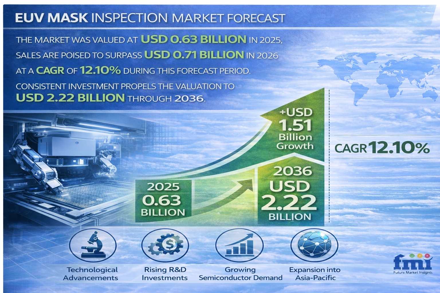
NEWARK, DE / ACCESS Newswire / March 27, 2026 / The global EUV mask inspection and pellicle monitoring systems market is entering a decisive growth phase as semiconductor manufacturers accelerate production at sub-3nm nodes. Valued at USD 0.63 billion in 2025, the market is projected to reach USD 0.71 billion in 2026 and expand significantly to USD 2.22 billion by 2036, registering a robust CAGR of 12.10% during the forecast period.
This rapid expansion reflects a fundamental shift in semiconductor manufacturing, where zero-defect lithography has become non-negotiable. As device geometries shrink and pattern complexity intensifies, even a single printable defect on an EUV mask can replicate across thousands of wafers, leading to catastrophic yield loss. Consequently, inspection systems are evolving into mission-critical infrastructure that ensures reticle integrity before high-volume production begins.
Get Access of Report Sample:
https://www.futuremarketinsights.com/reports/sample/rep-gb-32447
Market Value Analysis: Zero-Defect Mandates Driving Inspection Investments
Between 2026 and 2030, the EUV mask inspection market is expected to witness accelerated adoption as leading-edge foundries enforce full reticle inspection workflows. Traditional sampling-based approaches are no longer viable at advanced nodes, forcing lithography teams to implement comprehensive defect detection across entire mask surfaces.
Manufacturers are increasingly prioritizing:
Native-wavelength (actinic) inspection systems for accurate printability validation
Through-pellicle inspection technologies to detect hidden contamination
High-resolution defect classification platforms for multilayer structures
Integrated inspection workflows to prevent scanner downtime
Delays in deploying advanced inspection systems expose fabs to significant financial risk, as undetected defects can halt production lines and result in multi-million-dollar wafer losses.
From 2030 to 2036, market growth will be driven by the widespread adoption of High-NA EUV lithography and the increasing complexity of anamorphic mask designs, requiring even more advanced inspection capabilities.
Technology Evolution: Actinic Inspection and AI Redefine Defect Detection
The evolution of EUV mask inspection is being shaped by advancements in optical physics, vacuum engineering, and computational analytics. Conventional deep ultraviolet inspection tools are unable to detect phase defects within multilayer EUV masks, necessitating a transition to actinic (13.5 nm wavelength) systems.
Key innovations include:
Actinic EUV inspection systems for native-wavelength defect detection
Pellicle monitoring technologies enabling inspection without vacuum break
Machine learning algorithms for advanced defect classification and noise reduction
Die-to-database inspection for precise design-to-pattern validation
High-throughput plasma light sources improving scan speeds
A major challenge lies in balancing inspection accuracy with throughput. Native-wavelength systems offer unmatched precision but often require longer scan times, pushing manufacturers to invest in parallel inspection infrastructure.
An industry analyst notes:
"At sub-3nm nodes, inspection is no longer a supporting function-it defines yield. Foundries must inspect every reticle, every time, without compromise, fundamentally reshaping metrology investment strategies."
Reticle Integrity Becomes Central to Advanced Node Yield
As semiconductor manufacturing pushes into 3nm and 2nm territories, EUV mask inspection systems are emerging as indispensable components of the fabrication process. These systems enable:
Early detection of printable defects before wafer exposure
Identification of phase anomalies within multilayer reflectors
Monitoring of particle contamination through protective pellicles
Reduction of wafer scrap through proactive defect mitigation
Continuous reticle requalification during production cycles
This transformation is redefining competitive dynamics, where inspection capability directly impacts yield performance, fab utilization, and cost efficiency.
Segment Spotlight
Actinic EUV Inspection Leads Technology (34.0%)
Native-wavelength systems dominate due to their ability to detect phase defects invisible to optical tools.
Die-to-Database Inspection Dominates Mode (38.0%)
Advanced computational comparison ensures alignment with design intent in complex mask structures.
Mask Shop Qualification Leads Deployment (31.0%)
Pre-ship inspection ensures zero-defect delivery to wafer fabs.
Leading-Edge Foundries Lead End Use (42.0%)
High-volume manufacturers drive demand due to strict yield requirements.
3nm and 2nm Nodes Dominate Application (46.0%)
Advanced nodes require comprehensive inspection to maintain production viability.
Regional Insights: East Asia and North America Drive Market Expansion
Country |
CAGR (2026-2036) |
Key Growth Drivers |
|---|---|---|
Taiwan |
13.6% |
Dense foundry concentration and rapid node transitions |
South Korea |
12.8% |
Memory scaling and high-volume EUV adoption |
United States |
12.5% |
Reshoring initiatives and pilot line expansion |
Japan |
11.2% |
Strong merchant mask shop ecosystem |
Netherlands |
10.9% |
Core lithography innovation hub |
Germany |
10.6% |
Advanced optical component manufacturing |
China |
9.8% |
Domestic semiconductor self-sufficiency efforts |
Opportunities: Advanced Architectures and Computational Metrology Unlock Growth
Key opportunities shaping the market include:
Development of anamorphic inspection platforms for next-generation EUV systems
Carbon nanotube pellicle monitoring solutions for improved transmission analysis
AI-driven defect classification reducing false positives and improving throughput
Integration of inspection systems with lithography workflows for real-time feedback
Expansion of computational metrology software for faster data processing
These innovations are enabling scalable, high-precision inspection solutions tailored for increasingly complex semiconductor architectures.
Competitive Landscape: Technology Depth and Ecosystem Integration Define Leadership
The EUV mask inspection market is characterized by a highly concentrated group of specialized players with deep expertise in optics, metrology, and semiconductor process integration.
Leading companies include:
Lasertec Corporation
KLA Corporation
Carl Zeiss SMT GmbH
NuFlare Technology, Inc.
ASML Holding N.V.
Advantest Corporation
Hitachi High-Tech Corporation
Competitive differentiation is driven by:
Ability to deliver actinic (native-wavelength) inspection
Advanced defect detection and classification algorithms
Integration with mask shop and fab workflows
Throughput optimization for high-volume manufacturing
Future Outlook: Inspection Systems Become Core to EUV Manufacturing
Looking ahead to 2036, EUV mask inspection systems will become foundational to semiconductor fabrication at advanced nodes.
Key trends include:
Transition toward full reticle inspection without sampling
Increased reliance on actinic inspection for defect validation
Integration of AI-driven analytics for faster decision-making
Expansion of pellicle monitoring as a standard process step
Alignment of inspection performance with overall fab yield economics
As semiconductor manufacturers push toward 2nm and beyond, EUV mask inspection systems will evolve from supporting tools to critical enablers of high-yield, high-performance chip production-defining the future of advanced lithography.
For an in-depth analysis of evolving formulation trends and to access the complete strategic outlook for the EUV Mask Inspection and Pellicle Monitoring Systems Market through 2036, visit the official report page at: https://www.futuremarketinsights.com/reports/euv-mask-inspection-and-pellicle-monitoring-systems-market
Browse More Technology Industry Reports:
Security Labels Market - https://www.futuremarketinsights.com/reports/security-labels-market
Digital Experience Platform (DXP) Market - https://www.futuremarketinsights.com/reports/digital-experience-platform-market
Accounts Payable Automation Market - https://www.futuremarketinsights.com/reports/accounts-payable-automation-market
Harmonic Filter Market - https://www.futuremarketinsights.com/reports/harmonic-filter-market
Insurtech Market - https://www.futuremarketinsights.com/reports/insurtech-market
About Future Market Insights (FMI)
Future Market Insights (FMI) is a leading provider of market intelligence and consulting services, serving clients in over 150 countries. Headquartered in Delaware, USA, with a global delivery center in India and offices in the UK and UAE, FMI delivers actionable insights to businesses across industries including automotive, technology, consumer products, manufacturing, energy, and chemicals.
An ESOMAR-certified research organization, FMI provides custom and syndicated market reports and consulting services, supporting both Fortune 1,000 companies and SMEs. Its team of 300+ experienced analysts ensures credible, data-driven insights to help clients navigate global markets and identify growth opportunities.
For Press & Corporate Inquiries
Rahul Singh
AVP - Marketing and Growth Strategy
Future Market Insights, Inc.
+91 8600020075
For Sales - sales@futuremarketinsights.com
For Media - Rahul.singh@futuremarketinsights.com
For web - https://www.futuremarketinsights.com/
SOURCE: Future Market Insights, Inc.
View the original press release on ACCESS Newswire